
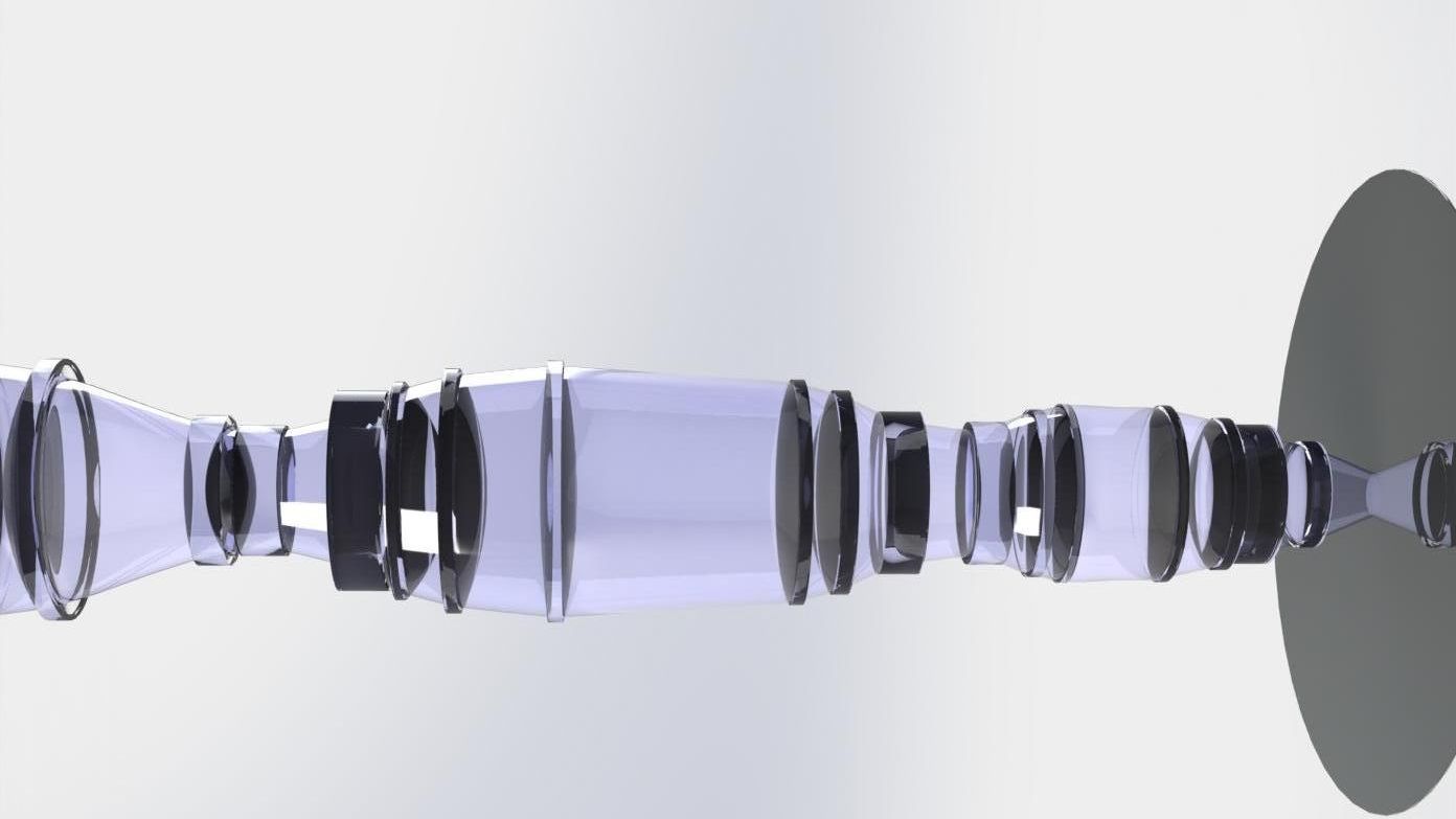

project specifics
- Magnification 5x (0.2x)
- Telecentric on image side
- FOV 22mm x 22 mm
- Diffraction limited
- CD < 0.4um (NA> 0.5)
- High CD uniformity (<2%)
- Useable DOF ~ 1 um
- Distortion < 100nm (maximum over field)
- Magnification needs to be adjustable using back-focus
- Order of magnitude 10 ppm
- Minimize magnification and focus errors due to short term temperature fluctuations within +/-0.1 degree
- Magnification change and focus due to pressure change is compensated using focus and back-focus only
"it is all about precision opto-mechanics."
Within Demcon focal we are very proud that we managed to design and realize this masterpiece.