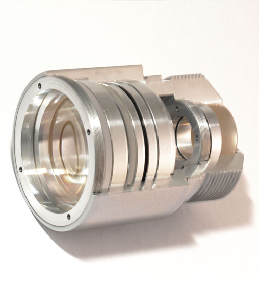
inspection system for light connectors.
A car is fitted with all kinds of lights, from headlights to lights on the dashboard. Each and every single one of these lights requires its own specific connector.
A car is fitted with all kinds of lights, from headlights to lights on the dashboard. Each and every single one of these lights requires its own specific connector.
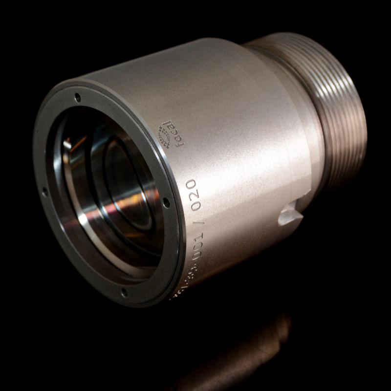
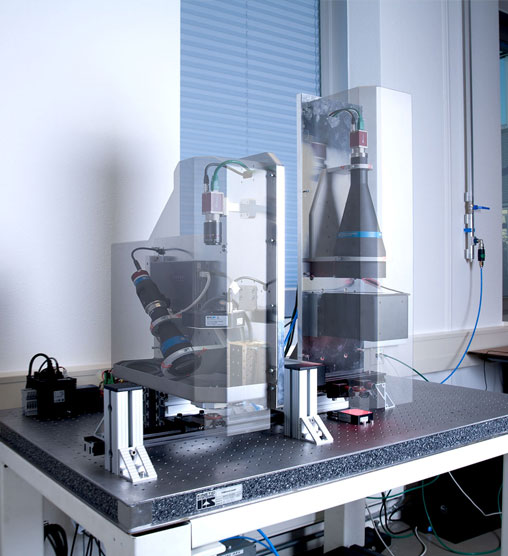
Projects for designing and creating lenses do not stop after assembly: lenses need to be qualified and tested against customer requirements.
We developed a UV laser beam delivery system for heat load experiments and wrinkle measurements.
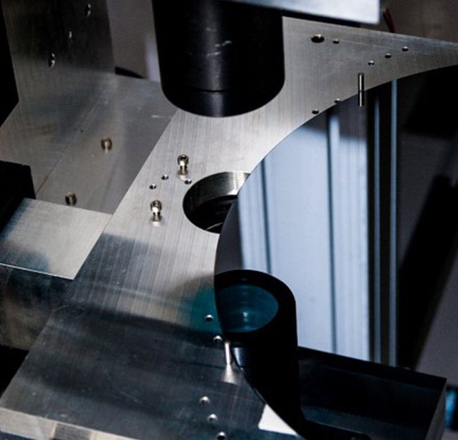
Accurate pre-alignment of wafers is key for each individual processing step. Contactless wafer edge measurement requires a dedicated vision system.
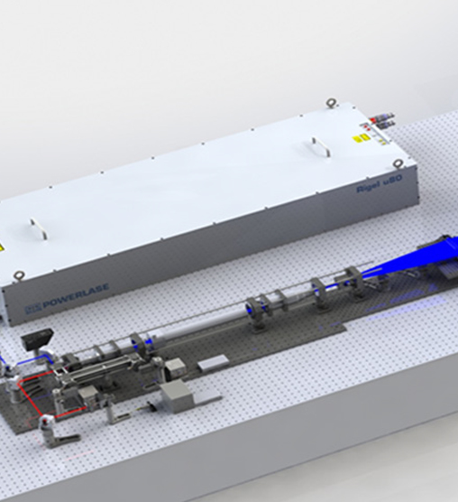
Laser annealing is growing rapidly in the semicon market. The elementary module for the laser annealing process is a laser beam delivery system that conditions the laser beam such that a uniform annealing is achieved over the surface.
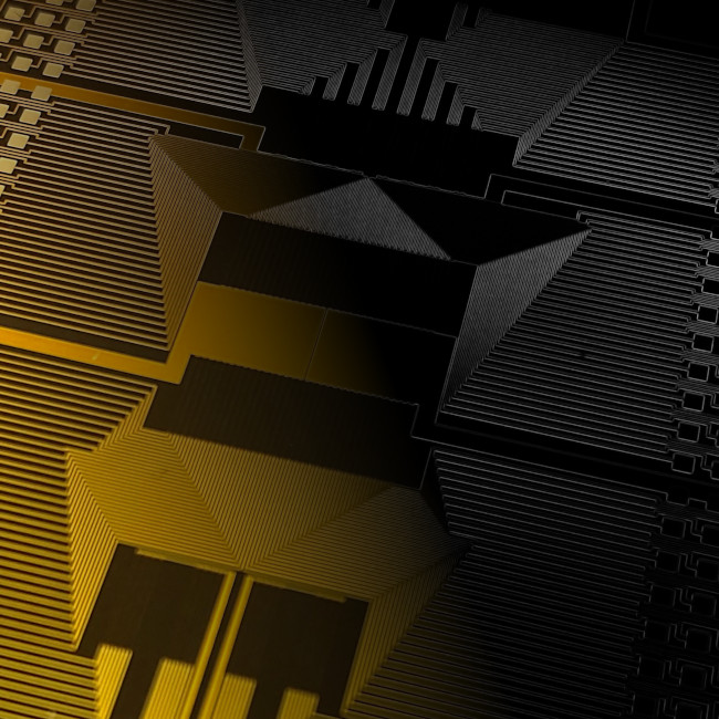
Wafer inspection and chip inspection require bespoke image hardware and analysis methods.